Silicon Wafers Manufacturing Business in India
A High-Tech Business Opportunity Most Entrepreneurs Overlook
There are few business concepts that combine technology, national strategy and pure scarcity like silicon wafers manufacturing. At the starting point of the supply chain of billions of dollars in semiconductors and electronic components that India imports annually is the silicon wafer—the ultra-thin disk of purified silicon that is the foundation of every chip, solar cell, and electronic device. But the domestic manufacturing sector is very underdeveloped. This opportunity is a rare, defensible and government-sanctioned opportunity for the right entrepreneur.
The international trend of chip sovereignty is more pronounced than ever. India is taking a big step to build a strong ecosystem for electronics manufacturing with silicon wafer production being a natural step. If you are in the solar panel industry, electronics or any type of research, the demand for solar panel makers is going to be great and increasing. This article explores the market rationale, the government incentives on offer, viable business ideas, and the case studies that demonstrate that this is a viable area for serious MSME participation.
Why Silicon Wafers Manufacturing Is a Smart Sector to Enter Right Now
The electronics manufacturing industry in India has expanded a lot faster than what was expected a decade ago. The defence electronics market is scaling at a rapid pace, as are mobile phones, consumer electronics, EVs and the solar panel market. All of these industries rely on semiconductors or silicon wafers for solar applications. Presently, India imports almost all its raw materials from Japan, Korea, Taiwan and Germany. Such a dependency exposes an opportunity, but also a vulnerability.
The government has made semiconductor and electronics self-reliance a top policy priority. The India Semiconductor Mission and PLI (Production Linked Incentive) scheme for electronics have been created specifically to curtail this import reliance. At the same time, the need has been bolstered by disruption of the global supply chain. To guarantee production pipelines, manufacturers are actively looking for wafer suppliers in India. In order to ensure production pipelines, Indian manufacturers are seeking wafer suppliers from within the country.
In the demand side, India’s solar energy target demands a huge amount of photovoltaic silicon wafers. The EV battery and power electronics market is another aspect of demand. A diverse and long-term buyer base is completed by research institutions, ISRO, DRDO and private defence electronics companies. A manufacturer that enters the market now and works to build quality and consistency has not only a market available, it is one guaranteed to expand.
Related Article: India’s Semiconductor Opportunity for MSMEs: Profitable Business Ideas
Government Policies and Incentives Supporting This Business
India Semiconductor Mission and PLI Scheme
The India Semiconductor Mission (ISM) under the Ministry of Electronics and Information Technology (MeitY) is offering financial assistance of up to 50% for semiconductor and display manufacturing units. That encompasses silicon wafer production. The PLI Scheme for Large Scale Electronics Manufacturing (LSE) also provides production-linked cash benefits for the production of domestic components.
MSME Schemes and Startup Benefits
With the Credit Guarantee Fund Trust for Micro and Small Enterprises (CGTMSE), loans with no collateral are available up to ₹2 crore. The Technology Upgradation Fund Scheme (TUFS), a scheme for technology-intensive manufacturing, is providing capital subsidy. Startup India initiative also provides tax benefits, quick compliance, and easier access to government procurement opportunities to first-time entrepreneurs.
Make in India and DPIIT Recognition
Make in India registration and recognition by the Department for Promotion of Industry and Internal Trade (DPIIT) opens up doors to preferential procurement opportunities, industrial zones and access to state level capital investment subsidies. Several state governments such as Gujarat, Telangana and Karnataka provide electronics manufacturing parks with plug and play facilities for industries related to the semiconductor industry.
Solar wafer producers can also leverage schemes under the Ministry of New and Renewable Energy (MNRE) which promotes domestic production of solar components under a scheme known as Approved List of Models and Manufacturers (ALMM), which ensures the use of domestically approved components in solar projects taken up by the government.
Business Ideas in Silicon Wafers Manufacturing for Indian Startups
1. Solar-Grade Silicon Wafer Production Unit
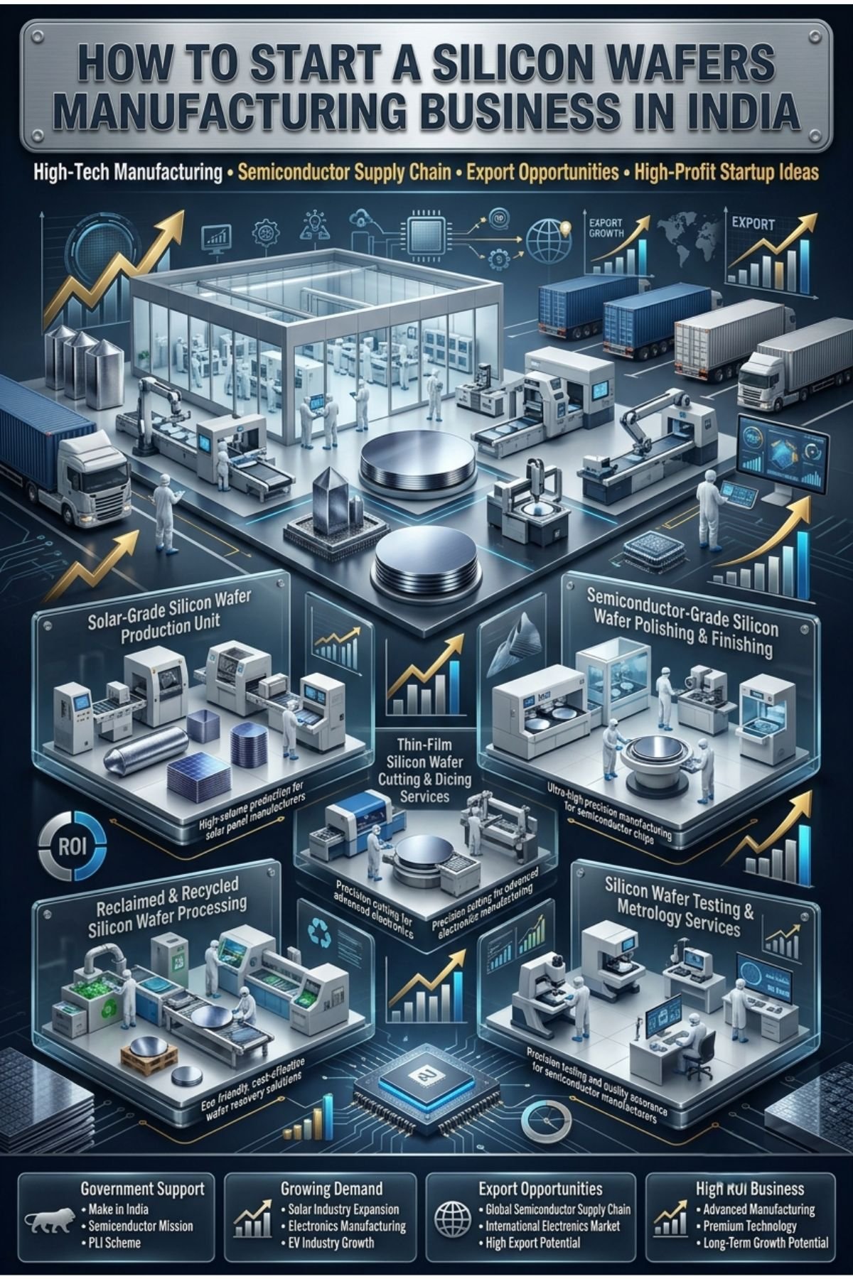
PV industry uses silicon wafers most extensively worldwide, and India is developing one of the world’s most ambitious solar energy programmes. A solar-grade silicon wafer manufacturing unit produces thin polycrystalline or monocrystalline wafers needed for the production of solar cells. The establishment of a mid-scale unit (50–100 MW/year of wafer production) requires investments in the wire-saw cutting line, cleaning and texturing lines and quality control system. The basic requirement of capital may vary from ₹4 crore to ₹8 crore depending upon the capacity and level of automation. The margins are good, though, because the solar panel manufacturers are keen to develop a more localised supply chain to meet the government’s domestic content quota. A key domestic supplier’s supply contract with 3-5 years of assured offtake can significantly de-risk the investment from day one.
2. Semiconductor-Grade Silicon Wafer Polishing and Finishing Unit
Explore This Book: Electroplating, Anodizing & Metal Treatment Handbook
3. Thin-Film Silicon Wafer Cutting and Dicing Services
Most small electronics manufacturers do not have the equipment to specialise in the task of dicing and precision cutting silicon wafers into individual chips or custom sizes. A cleanroom environment is required, along with diamond-blade or laser dicing machines and a requirement for particle control. Investment amount is from ₹1.5 crores to ₹3 crore. It has a service-based business model; i.e., it makes money per wafer processed, not based on product sales, and this reduces risk of inventory. It is a good model for electronics clusters such as Bengaluru, Pune, Hyderabad and Chennai, where the concentration of electronics manufacturers provides a constant stream of orders for dicing. The main competitive parameters in this business are turnaround time and yield rate.
4. Reclaimed and Recycled Silicon Wafer Processing
A large amount of silicon wafers is rejected, broken or used during semiconductor fabrication. In reclaimed wafer processing, we retrieve these wafers, polish them to improve surface quality, and then sell them for non-critical uses such as R&D testing, education labs, or low-grade sensor manufacturing. This circular economy model is slowly making its way to the planet because of its dramatic reduction in raw material cost. The demand for cheap and recycled wafers is steady in India, a country where research institutes, IITs, and private electronics research labs are booming. The investment is comparatively low, somewhere between ₹80 lakhs and ₹1.5 crores, so is a good place for first generation entrepreneurs to start into this business with a lesser risk involved.
5. Silicon Wafer Testing and Metrology Services
With the increase of silicon wafer manufacturing in India, the demand for independent quality verification also increases. Additionally, A silicon wafer testing and metrology company provides various wafer characterization services such as wafer resistivity, thickness uniformity, surface roughness and defect density. Moreover, Investment is needed for 4 point probe systems, atomic force microscopy (AFM) and surface profilometers and clean room space. The investment is in between ₹1.5 crore to ₹2.5 crore. Furthermore, We will generate revenue through testing contracts with wafer manufacturers, solar cell manufacturers, and R&D labs. Therefore, Due to maturing Indian semiconductor ecosystem and the shortening of supply chains, testing services will become a regulatory and quality necessity and become an annuity-like business model for the first movers in the domain.
Import–Export Opportunity Analysis for Silicon Wafer Startups
In addition, India is an importer of silicon wafer in bulk amount. Moreover, Leading suppliers include Japan (Shin-Etsu, Sumco), South Korea, Taiwan and Germany. The import bill is in crores of rupees every year. However, When a domestic manufacturer is able to meet the quality requirements, especially SEMI (Semiconductor Equipment and Materials International) certification, then there is a tremendous opportunity to take away the imports and generate a domestic market share at competitive prices.
Moreover, On the export side, Indian manufacturers that build quality-certified manufacturing plants will be able to tap markets in Southeast Asia, the Middle East, and Africa, where the semiconductor and solar industries are expanding but wafer production remains limited. Furthermore, As the countries like Vietnam, Bangladesh and Sri Lanka are developing electronics manufacturing capability, they would welcome a consistent supplier from India. Export credit insurance and export credit financing assistance are provided by EXIM Bank of India and ECGC (Export Credit Guarantee Corporation) to the manufacturers who are going for export markets. Meanwhile, Make in India brand is gaining traction in the manufacturing corridors of the world and the semiconductor adjacent export story has excellent positioning.
Further, the government and defence sectors will automatically trust BIS-certified companies that meet wafer quality standards, both in national operations and in government-to-government trade contracts. This generates a dual-market approach – home-grown import substitution and tactical export incursion – that ensures a more stable business climate, lessening the impact of any one market fluctuation.
Get Detailed Project Report (DPR): Silicon Metal Manufacturing Plant Report
Indian MSME Success Stories in the Semiconductor and Electronics Component Space
Moschip Technologies – Hyderabad
Moschip Technologies was established by K. Ramachandra Reddy who became one of the few home-grown semiconductors design and fabrication-adjacent companies in India. The promoter’s obsession with micro semiconductors as opposed to competing against the giants from around the world became the company’s competitive strategy. New entrepreneurs learn that, in high tech manufacturing, specialization and special customer relationships are more important than scale. For Indian MSMEs in the electronics segment, the tried and tested formula for success is to begin with a narrow range of products and gradually expand into new ones.
SPEL Semiconductor – Chennai
Rajeswari Viswanath promoted SPEL Semiconductor, making it India’s first indigenous semiconductor packaging and testing plant with support from institutional investors. The company’s success has proven that an MSME in India can compete with the big multinationals, provided it has the necessary expertise, time (patient capital), and quality. The success of SPEL proves that, if handled with discipline and nurtured with a sustained customer relationship, the semiconductor supply chain, comprising wafer related services and component processing, is commercially viable in India.
HCL Hardware (Early Era) – A Model of Technology Manufacturing Ambition
Certainly, HCL has come a long way, but its early hardware manufacturing days under Shiv Nadar have taught me a valuable lesson: India’s tech entrepreneurs who took a punt on hardware manufacturing when it didn’t appear to make sense often got it right when it came to the market. Moreover, In today’s world, where the MSME entrepreneur is the frontrunner, the silicon wafer industry is all set to be a similar moment. The market demand, policy support, and infrastructure are now aligned with each other in a way that they weren’t 5 years ago. Therefore, People who come in early, establish quality systems, and stick with it will be in a better position to create businesses with long-lasting value.
How NPCS Can Help You Enter the Silicon Wafers Business
We at Niir Project Consultancy Services (NPCS) offer professional consulting for new industry/business startup for the preparation of Market Survey cum Detailed Techno-Economic Feasibility Reports (DPRs). Our reports consist of manufacturing processes, market research and demand analysis, process flow diagrams, product mix and planning, capacity planning, machinery and raw material details, complete project financials, and profitability analysis. Our goal is to give entrepreneurs the information and data they need to determine whether a project is viable, profitable and scalable before they commit their capital.
In a technically challenging industry such as silicon wafers manufacturing, it is not a luxury, but a necessity to have knowledge of the process economics, machinery sourcing, raw material specifications and quality compliance requirements to make the difference between a successful plant and a costly misstep. Entrepreneurs receive the clarity needed to make informed investment decisions, and approach lenders and investors with valid documentation with our feasibility reports.
Your investment deserves the right opportunity
Silicon Wafers Manufacturing: Key Business Parameters at a Glance
| Business Model | Estimated Investment | Key Market / Buyer |
| Solar-Grade Wafer Production | ₹4 – ₹8 Crore | Solar Cell & Panel Manufacturers |
| Semiconductor Wafer Polishing Unit | ₹2 – ₹4 Crore | PCB Makers, MEMS, Research Labs |
| Wafer Dicing & Cutting Services | ₹1.5 – ₹3 Crore | Electronics Clusters, Chip Makers |
| Reclaimed Wafer Processing | ₹80 Lakh – ₹1.5 Crore | IITs, R&D Labs, Low-Grade Electronics |
| Wafer Testing & Metrology | ₹1.5 – ₹2.5 Crore | Wafer Mfrs, Solar Cos, Research Institutes |
FAQ: Silicon Wafers Manufacturing Business in India
1. What is the minimum investment required to start a silicon wafer business in India?
The kind of entry you require depends upon the type of business plan. An entry-point unit on processed wafer can start from Rs.80 Lakh to 1.5 Cr. A serious wafer unit with reasonable capacity can be put up at Rs. 4 to 8 Cr, on which you may get Govt support and CGTMSE collateral-free assistance that effectively cuts down equity contribution for eligible MSME.
2. Do I need a cleanroom facility to start this business?
Most silicon wafer processing operations – including polishing, dicing, and testing – require a cleanroom environment classified as ISO Class 6 or better. The cleanroom is a significant part of the capital investment. On the flip side, the specifications for reclaimed wafer processing for the educational and R&D markets may not be as strict as those for the production of semiconductor devices.
3. What are the key raw materials for silicon wafer manufacturing?
The main feedstock material will be polysilicon or monocrystalline silicon ingots, which currently come from China, Germany, and the USA. We need wire for wire cutting, polishing slurry made of a silicon carbide (SiC) compound, and chemicals for etching and texturing. In a further stage we will consider producing locally polysilicon and other needed raw materials. In the short run it is important to guarantee imports and having a few providers to prevent an overdependency.
4. What quality certifications are needed to sell silicon wafers in India and globally?
SEMI certification from SEMI International, the global semiconductor industry standards body, serves as the primary quality benchmark that electronics and semiconductor manufacturers worldwide recognize. BIS certification is important for government and defence procurement in India. For solar wafer applications, solar panel manufacturers typically require photovoltaic cells to comply with IEC standards.
5. Which government schemes directly support silicon wafer manufacturing startups?
Under the India Semiconductor Mission MeitY supports projects up to 50% project cost. The PLI Scheme for Electronics Manufacturing provides with incentives linked to production. CGTMSE gives collateral free loans up to 2 crores to applicants from the MSME category. The state governments of Gujarat, Telangana, Karnataka, Tamil Nadu come with their own incentive schemes under electronics manufacturing park to provide with additional capital subsidy along with the required infrastructure on plug-and-play basis.
6. How long does it take to set up a silicon wafer manufacturing unit and start commercial operations?
For a wafer dicing or testing services unit, setup can be completed in 12 to 18 months from project inception to first commercial order. A full solar-grade wafer production facility typically requires 24 to 36 months for land acquisition, plant construction, equipment procurement, cleanroom commissioning, and quality certification. We strongly recommend preparing a detailed project report (DPR) with realistic timelines and financial projections before committing capital.
Conclusion: The Time to Enter Is Now
Wafer manufacturing – is at the core of what is perhaps India’s biggest push for industrial transformation. Not only has the government set aside billions of dollars in investment and support to create a robust semiconductor ecosystem in the country, the private sector is also lining up. But on the first rung of this complex ecosystem, in the making of wafers, local entrepreneurs remain woefully few in number.
If you as founders can accept putting resources into technology capability, quality systems, and customer relationships of significance over time, there is likely no better sector for this mix of powerful policy tailwinds, a paucity of local competition, abundant and diverse customer demand, and an appetite at the state level for partners who will build toward national self-sufficiency. From wafers to dicing, to polishing, to testing, the underlying business case makes an overwhelming amount of sense right now.(Silicon Wafers Manufacturing Business in India)
Success in a capital-intensive, high-technology undertaking hinges, as always, on meticulous planning. Conduct a feasibility study, evaluate process economics, secure your first three customers before laying the first brick, and apply as early as possible for available government grants. Those who tread prudently but swiftly over the next few years will have a locked position in one of India’s most critical sectors.