
 Bajaj Steel Industries
 Tata Steel
 JSW Steel
 ITC (Agri Business Division)
 Godrej & Boyce
 Aditya Birla Management Corporation
 Grasim Industries (Century Rayon)
 Thermax (Chemical Division)
Electronics makers, LED lighting firms and automotive suppliers all need bare boards, and many still import them. A printed circuit board plant consultant helps you turn that gap into a workable factory plan. The plant images, etches and plates copper-clad laminates into single, double-sided and multilayer boards. NPCS works with entrepreneurs and investors on capacity, technology, effluent handling and finance, so your decisions rest on a clear project report.
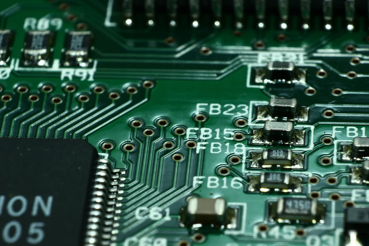
Printed Circuit Board Plant at a Glance
| Typical capacity | ~2,000–50,000 sq m/month |
|---|---|
| Land | ~2–6 acres |
| Power load | ~1–5 MW |
| Water | High (ETP or ZLD) |
| Manpower | ~80–400 |
| Indicative investment | ~₹20–300 crore |
Investment basis: multilayer lines at the top end; excludes land.
Figures are indicative ranges. Your project report works them out for your capacity and location.
Market Demand for Printed Circuit Boards in India
Demand for bare boards in India is pushed by the electronics manufacturing drive and by import substitution. Buyers are mainly EMS companies, LED and appliance makers, and automotive and industrial OEMs. Export potential is medium, so most early sales are domestic. Demand isn't seasonal, which helps steady production planning. Established manufacturing is concentrated in a few regions.
- Delhi-NCR (Noida)
- Karnataka
- Tamil Nadu
- Gujarat
- Maharashtra
Printed Circuit Board Types You Can Make
Aluminium-backed LED boards and single-sided boards suit lighting and power customers, and they need a lighter line. Double-sided PTH and multilayer boards serve telecom, automotive and industrial controls. Flexible PCBs are a separate specialty. Choose the variants that match the buyers you can reach first.
- Single-sided, double-sided PTH, multilayer (4–12 layers), aluminium-backed LED boards, flexible PCBs
Printed Circuit Board Plant Process
The printed circuit board plant process starts with drilling and plating through holes, then moves to dry film imaging and etching. Multilayer boards add a lamination stage. After that, the boards get solder mask, a surface finish such as HASL or ENIG, and legend printing. Quality is controlled at several points rather than only at the end. Electrical testing, AOI, plating thickness and solderability checks are typical, and boards are judged against IPC-A-600 acceptability. Single and double-sided lines suit LED and power boards, while multilayer lines need higher capex.
- Drilling
- Plating through holes
- Imaging (dry film)
- Etching
- (lamination for multilayer)
- Solder mask
- Surface finish (HASL, ENIG)
- Legend printing
- Electrical testing
- Routing and packing
Raw Materials and Machinery for a PCB Plant
Copper-clad laminates in FR4, CEM or aluminium are the main input, and they are largely imported from China and Taiwan. Dry film, plating and etching chemicals, solder mask and legend inks are sourced domestically and from abroad. Among the machines, CNC drilling, plating lines, laser direct imaging and the flying-probe tester shape yield most.
- CNC drilling
- Plating lines
- Imaging (laser direct imaging)
- Etching lines
- Lamination press
- Solder mask coater
- Surface finish line
- Flying-probe tester
- Router
- ETP
Printed Circuit Board Plant Licence and Approvals
Approvals start with business registration and a factory licence, followed by consent to establish from the State Pollution Control Board before construction. Etching and plating place the plant in the Red category. Hazardous waste authorisation is also needed, and ZLD applies in many clusters. Consent to operate follows once the effluent system is in place. No BIS QCO applies to this product.
- Business registration and factory licence
- Consent to establish before construction
- Hazardous waste authorisation
- Consent to operate after commissioning
| Pollution category | PCB manufacturing with etching and plating: Red (metal surface treatment, CPCB S.No. 101.1) |
|---|---|
| HSN code | 8534 (printed circuits) |
| GST | 18% |
| BIS / quality control order | No QCO |
| Other licences | Hazardous waste authorisation; ZLD in many clusters; factory licence |
Choosing the Right PCB Plant Size
Plant size changes the project more in PCB fabrication than in most industries. Indicative capacity runs from about 2,000 to 50,000 sq m/month, with investment from about ₹20–300 crore excluding land. A smaller single or double-sided unit for LED boards needs far less capital. Multilayer lines sit at the top end. Many promoters start small with proven board types, then add layers once yields and customers are steady.
Quality Standards for Printed Circuit Boards
No QCO applies, so buyers set the quality bar themselves. EMS companies and automotive OEMs typically expect boards built to IPC-A-600 acceptability, backed by electrical test and AOI records. Plating thickness and solderability data also count in supplier audits. Plan your inspection equipment and documentation at the design stage, because adding them later disrupts production and delays approvals from demanding customers.
Government Schemes and Project Finance for a PCB Plant
The Electronics Component Manufacturing Scheme (ECMS) covers PCBs, and SPECS and state electronics policies may also apply. Eligibility depends on each scheme's current terms. NPCS reports are used for bank loans and programmes such as MSME schemes, subject to each lender's requirements. A bankable project report with realistic yields and effluent costs strengthens your application.
What Decides Success in a PCB Plant
Good operators focus on yield, quick-turn service and strong effluent management. The main risks are Chinese competition, chemical effluent and dependence on imported laminates. Copper-bearing sludge and spent etchant can be recovered, which eases disposal and adds value.
- Hold yield and quality steady
- Offer quick-turn delivery
- Budget early for effluent treatment
- Plan laminate supply and stock
How NPCS Helps You Set Up a PCB Plant
NPCS supports the decisions that shape a PCB project: capacity, single or multilayer technology, machinery selection and vendors. Our team also guides plant layout, the approvals sequence and finance planning. We prepare detailed and bankable project reports and help with installation and commissioning assistance, so your plan matches your budget, location and customers.
NPCS's published client list records 3 assignments on printed circuit board projects between 2021 and 2025 for clients in 3 states, including detailed project reports, bankable project reports and techno-economic feasibility studies.
What Your Printed Circuit Board Plant Project Report Covers
- Project introduction and BIS specifications
- Manufacturing process with flow sheet
- Market survey (demand, imports/exports, existing units)
- Personnel
- Plant and machinery with suppliers
- Land and building with layout
- Raw materials with sources and rates
- Financials (project cost, working capital, cost of production, profitability, break-even, 5–10 year cash flow, projected balance sheet, IRR/NPV/payback)
Printed Circuit Board Plant: Frequently Asked Questions
What is the printed circuit board plant setup cost in India?
Indicative investment runs from about ₹20–300 crore, excluding land. Multilayer lines sit at the top end. Your actual cost depends on capacity, technology and location, which a project report works out in detail.
Which pollution category applies to a PCB plant?
PCB manufacturing with etching and plating falls in the Red category under CPCB S.No. 101.1. You'll also need hazardous waste authorisation, and ZLD applies in many clusters.
How much land and power does a PCB plant need?
A plant typically needs about 2–6 acres and a power load of about 1–5 MW, depending on capacity. Water demand is high, so plan for an ETP or ZLD system.
How to start a printed circuit board plant business?
Begin by fixing board types, capacity and target buyers, then prepare a project report. Next, secure land, consent to establish and funding, and finalise machinery. Consent to operate comes after commissioning.
How can NPCS help with a PCB project report?
NPCS prepares detailed project reports, bankable reports and feasibility studies covering process, machinery, approvals and financials. You can share your capacity and location, and our team will tailor the report.